Visible to Intel only — GUID: hnj1476724450050
Ixiasoft
Product Discontinuance Notification
1. Introduction to Intel® FPGA SDK for OpenCL™ Pro Edition Best Practices Guide
2. Reviewing Your Kernel's report.html File
3. OpenCL Kernel Design Concepts
4. OpenCL Kernel Design Best Practices
5. Profiling Your Kernel to Identify Performance Bottlenecks
6. Strategies for Improving Single Work-Item Kernel Performance
7. Strategies for Improving NDRange Kernel Data Processing Efficiency
8. Strategies for Improving Memory Access Efficiency
9. Strategies for Optimizing FPGA Area Usage
10. Strategies for Optimizing Intel® Stratix® 10 OpenCL Designs
11. Strategies for Improving Performance in Your Host Application
12. Intel® FPGA SDK for OpenCL™ Pro Edition Best Practices Guide Archives
A. Document Revision History for the Intel® FPGA SDK for OpenCL™ Pro Edition Best Practices Guide
2.1. High-Level Design Report Layout
2.2. Reviewing the Summary Report
2.3. Viewing Throughput Bottlenecks in the Design
2.4. Using Views
2.5. Analyzing Throughput
2.6. Reviewing Area Information
2.7. Optimizing an OpenCL Design Example Based on Information in the HTML Report
2.8. Accessing HLD FPGA Reports in JSON Format
4.1. Transferring Data Via Intel® FPGA SDK for OpenCL™ Channels or OpenCL Pipes
4.2. Unrolling Loops
4.3. Optimizing Floating-Point Operations
4.4. Allocating Aligned Memory
4.5. Aligning a Struct with or without Padding
4.6. Maintaining Similar Structures for Vector Type Elements
4.7. Avoiding Pointer Aliasing
4.8. Avoid Expensive Functions
4.9. Avoiding Work-Item ID-Dependent Backward Branching
5.1. Best Practices for Profiling Your Kernel
5.2. Instrumenting the Kernel Pipeline with Performance Counters (-profile)
5.3. Obtaining Profiling Data During Runtime
5.4. Reducing Area Resource Use While Profiling
5.5. Temporal Performance Collection
5.6. Performance Data Types
5.7. Interpreting the Profiling Information
5.8. Profiler Analyses of Example OpenCL Design Scenarios
5.9. Intel® FPGA Dynamic Profiler for OpenCL™ Limitations
8.1. General Guidelines on Optimizing Memory Accesses
8.2. Optimize Global Memory Accesses
8.3. Performing Kernel Computations Using Constant, Local or Private Memory
8.4. Improving Kernel Performance by Banking the Local Memory
8.5. Optimizing Accesses to Local Memory by Controlling the Memory Replication Factor
8.6. Minimizing the Memory Dependencies for Loop Pipelining
8.7. Static Memory Coalescing
Visible to Intel only — GUID: hnj1476724450050
Ixiasoft
3.2. Global Memory Interconnect
The ability to maximize memory bandwidth for read and write accesses is crucial for high performance computing. Various types of modules for reading from and writing to global memory can exist in an OpenCL™ system. These modules are called load-store units (LSUs).
Unlike a GPU, an FPGA can build any custom LSU that is best suited for the memory access pattern that the compiler infers for your application. As a result, your ability to write OpenCL code that selects the ideal LSU types for your application might help improve the performance of your design significantly.
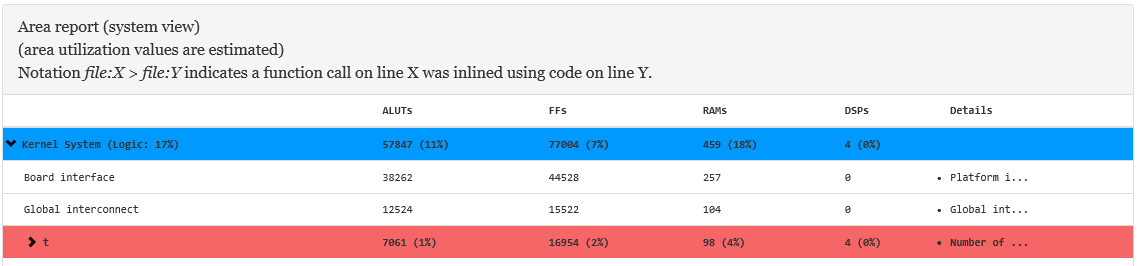
When reviewing the HTML area report of your design, the values in the Global interconnect entry at the system level represents the size of the global memory interconnect.
Figure 36. HTML Area Report Showing the Size of the Global Memory Interconnect in an OpenCL Design
In the HTML report, the system view of the System Viewer depicts global memory interconnects as loads (LD), stores (ST), and connections (gray lines).
Figure 37. System Viewer (System View) Result of Global Memory Interconnects in an OpenCL Design

The Intel® FPGA SDK for OpenCL Offline Compiler selects the appropriate type of LSU for your OpenCL system based on the memory access pattern of your design. Example LSU types include contiguous access (or consecutive access) and burst-interleaved access. Contiguous Memory Access and Global Memory Partitions illustrate the difference in access patterns between contiguous and burst-interleaved memory accesses, respectively.