Visible to Intel only — GUID: eis1411545767576
Ixiasoft
1. About Floating-Point IP Cores
2. FP_ACC_CUSTOM Intel® FPGA IP or Floating Point Custom Accumulator Intel® FPGA IP Core
3. ALTFP_ADD_SUB IP Core
4. ALTFP_DIV IP Core
5. ALTFP_MULT IP Core
6. ALTFP_SQRT
7. ALTFP_EXP IP Core
8. ALTFP_INV IP Core
9. ALTFP_INV_SQRT IP Core
10. ALTFP_LOG
11. ALTFP_ATAN IP Core
12. ALTFP_SINCOS IP Core
13. ALTFP_ABS IP Core
14. ALTFP_COMPARE IP Core
15. ALTFP_CONVERT IP Core
16. FP_FUNCTIONS Intel® FPGA IP or Floating Point Functions Intel® FPGA IP Core
17. Floating-Point IP Cores User Guide Document Archives
18. Document Revision History for the Floating-Point IP Cores User Guide
1.1. List of Floating-Point IP Cores
1.2. Installing and Licensing Intel® FPGA IP Cores
1.3. Design Flow
1.4. Upgrading IP Cores
1.5. Floating-Point IP Cores General Features
1.6. IEEE-754 Standard for Floating-Point Arithmetic
1.7. Non-IEEE-754 Standard Format
1.8. Floating-Points IP Cores Output Latency
1.9. Floating-Point IP Cores Design Example Files
1.10. VHDL Component Declaration
1.11. VHDL LIBRARY-USE Declaration
2.1. FP_ACC_CUSTOM Intel® FPGA IP or Floating Point Custom Accumulator Intel® FPGA IP Features
2.2. FP_ACC_CUSTOM Intel® FPGA IP or Floating Point Custom Accumulator Intel® FPGA IP Output Latency
2.3. FP_ACC_CUSTOM Intel® FPGA IP Resource Utilization and Performance
2.4. FP_ACC_CUSTOM Intel® FPGA IP or Floating Point Custom Accumulator Intel® FPGA IP Signals
2.5. FP_ACC_CUSTOM Intel® FPGA IP or Floating Point Custom Accumulator Intel® FPGA IP Parameters
15.1. ALTFP_CONVERT Features
15.2. ALTFP_CONVERT Conversion Operations
15.3. ALTFP_CONVERT Output Latency
15.4. ALTFP_CONVERT Resource Utilization and Performance
15.5. ALTFP_CONVERT Design Example: Convert Double-Precision Floating-Point Format Numbers
15.6. ALTFP_CONVERT Signals
15.7. ALTFP_CONVERT Parameters
16.1. FP_FUNCTIONS Intel® FPGA IP or Floating Point Functions Intel® FPGA IP Features
16.2. FP_FUNCTIONS Intel® FPGA IP or Floating Point Functions Intel® FPGA IP Output Latency
16.3. FP_FUNCTIONS Intel® FPGA IP or Floating Point Functions Intel® FPGA IP Target Frequency
16.4. FP_FUNCTIONS Intel® FPGA IP or Floating Point Functions Intel® FPGA IP Combined Target
16.5. FP_FUNCTIONS Intel® FPGA IP Resource Utilization and Performance
16.6. FP_FUNCTIONS Intel® FPGA IP Signals
16.7. FP_FUNCTIONS Intel® FPGA IP Parameters
Visible to Intel only — GUID: eis1411545767576
Ixiasoft
3.5.1. ALTFP_ADD_SUB Design Example: Understanding the Simulation Results
The simulation waveform in this design example is not shown in its entirety. Run the design example files in the ModelSim* - Intel® FPGA Edition software to see the complete simulation waveforms.
Figure 15. ALTFP_ADD_SUB Simulation Waveform
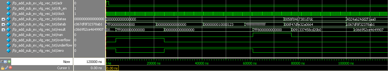
This design example implements a floating-point adder for the addition of double-precision format numbers. All the optional input ports (clk_en and aclr) and optional output ports (overflow, underflow, zero, and nan) are enabled.
In this example, the output latency of the multiplier is set to 7 clock cycles. Every addition result appears at the result[] port 7 clock cycles after the input values are captured on the dataa[] and datab[] ports.
The following lists the inputs and corresponding outputs obtained from the simulation waveform.
| Time | Event |
|---|---|
| 0 ns, start-up | dataa[] value: 0000 0000 0000 0000h datab[] value: 7FF0 0000 0000 0000h Output value: All values seen on the output port before the 7th clock cycle are merely due to the behavior of the system during startup and should be disregarded. |
| 4250 ns | Output value: 7FF0 0000 0000 0000h Exception handling ports: overflow asserts The addition of zero at the input port dataa[], and infinity value at the input port datab[] results in infinity value. |
| 40,511 ns | dataa[] value: 0000 0000 0000 0000h datab[] value: 0000 0000 1000 0123h The is the addition of a zero and a denormal value. |
| 43,750 ns | Output value: 0000 0000 0000 0000h Exception handling ports: zero remains asserted. Denormal inputs are not supported and are forced to zero before addition takes place.This results in a zero. |