Visible to Intel only — GUID: xva1487174954859
Ixiasoft
1. Overview of the Early Power Estimator for Intel® Stratix® 10 Devices
2. Setting Up the Early Power Estimator for Intel® Stratix® 10 Devices
3. Early Power Estimator for Intel® Stratix® 10 Graphical User Interface
4. Early Power Estimator Worksheets for Intel® Stratix® 10 Devices
5. Factors Affecting the Accuracy of the Early Power Estimator
6. Document Revision History for Early Power Estimator for Intel® Stratix® 10 FPGAs User Guide
A. Measuring Static Power
4.1. Intel® Stratix® 10 EPE - Common Worksheet Elements
4.2. Intel® Stratix® 10 EPE - Main Worksheet
4.3. Intel® Stratix® 10 EPE - Logic Worksheet
4.4. Intel® Stratix® 10 EPE - RAM Worksheet
4.5. Intel® Stratix® 10 EPE - DSP Worksheet
4.6. Intel® Stratix® 10 EPE - Clock Worksheet
4.7. Intel® Stratix® 10 EPE - PLL Worksheet
4.8. Intel® Stratix® 10 EPE - I/O Worksheet
4.9. Intel® Stratix® 10 EPE - I/O-IP Worksheet
4.10. Intel® Stratix® 10 EPE - XCVR Worksheet
4.11. Intel® Stratix® 10 EPE - HPS Worksheet
4.12. Intel® Stratix® 10 EPE - HBM Worksheet
4.13. Intel® Stratix® 10 EPE - Thermal Worksheet
4.14. Intel® Stratix® 10 EPE - Report Worksheet
4.15. Intel® Stratix® 10 EPE - Intel® Enpirion® Worksheet
Visible to Intel only — GUID: xva1487174954859
Ixiasoft
4.9. Intel® Stratix® 10 EPE - I/O-IP Worksheet
Each row in the I/O-IP worksheet of the Early Power Estimator (EPE) for Intel® Stratix® 10 devices represents a design module. You can use the I/O-IP worksheet to instantiate external memory interface and HPS IPs supported in Intel® Stratix® 10 devices. The I/O-IP worksheet populates other EPE worksheets with resources used by a selected IP.
Analog I/O power and digital power of hard memory controllers and HPS IPs entered on this tab are reported in the Analog Power and Digital Power fields of the I/O worksheet. If the IP uses other resource types (for example Logic or PLL), the power is reported on the corresponding worksheet.
Figure 17. I/O-IP Worksheet of the Early Power Estimator
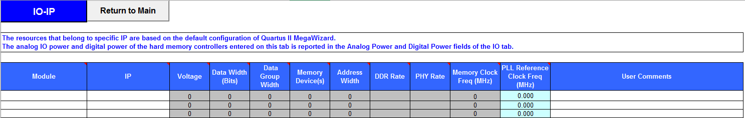
I/O-IP Worksheet Information
| Column Heading | Description |
|---|---|
| Module | Specify a name for the IP in this column. The module name depends on the selected IP type. It helps to cross-reference each IP module and its corresponding auto-populated entries on other worksheets. |
| IP | Specifies the name of the IP in the design. |
| Voltage | Specifies the I/O voltage of the signaling between periphery device and interface. |
| Data Width (Bits) | Specifies the interface data width of the specific IP (in bits). |
| Data Group Width | Specifies the number of DQ pins per data group. |
| Memory Device(s) | Specifies the number of memory devices connected to the interface. |
| Address Width | Specifies the address width. This value is used to derive the total number of address pins required. |
| DDR Rate | Specifies the clock rate of user logic. Determines the clock frequency of user logic in relation to the memory clock frequency. For example, if the memory clock sent from the FPGA to the memory device is toggling at 800MHz, a "Quarter rate" interface means that the user logic in the FPGA runs at 200MHz. |
| PHY Rate | Specifies the clock rate of PHY logic. Determines the clock frequency of PHY logic in relation to the memory clock frequency. For example, if the memory clock sent from the FPGA to the memory device is toggling at 800MHz, a "Quarter rate" interface means that the PHY logic in the FPGA runs at 200MHz. |
| Memory Clock Freq (MHz) | Specifies the frequency of memory clock (in MHz). |
| PLL Reference Clock Freq (MHz) | Specifies the PLL Reference Clock Frequency (in MHz). |
| User Comments | Enter any comments. This is an optional entry. |