4.13. Intel® Stratix® 10 EPE - Thermal Worksheet
The Thermal worksheet of the Early Power Estimator (EPE) for Intel® Stratix® 10 devices allows you to enter temperature requirements for your design and displays thermal power and thermal analysis information.
To enable thermal calculations, you must select one of the devices that support thermal calculations, on the Main worksheet. Also on the Main worksheet, you must set Power Characteristics to Maximum, and Junction Temp Mode to Detailed Thermal Model.
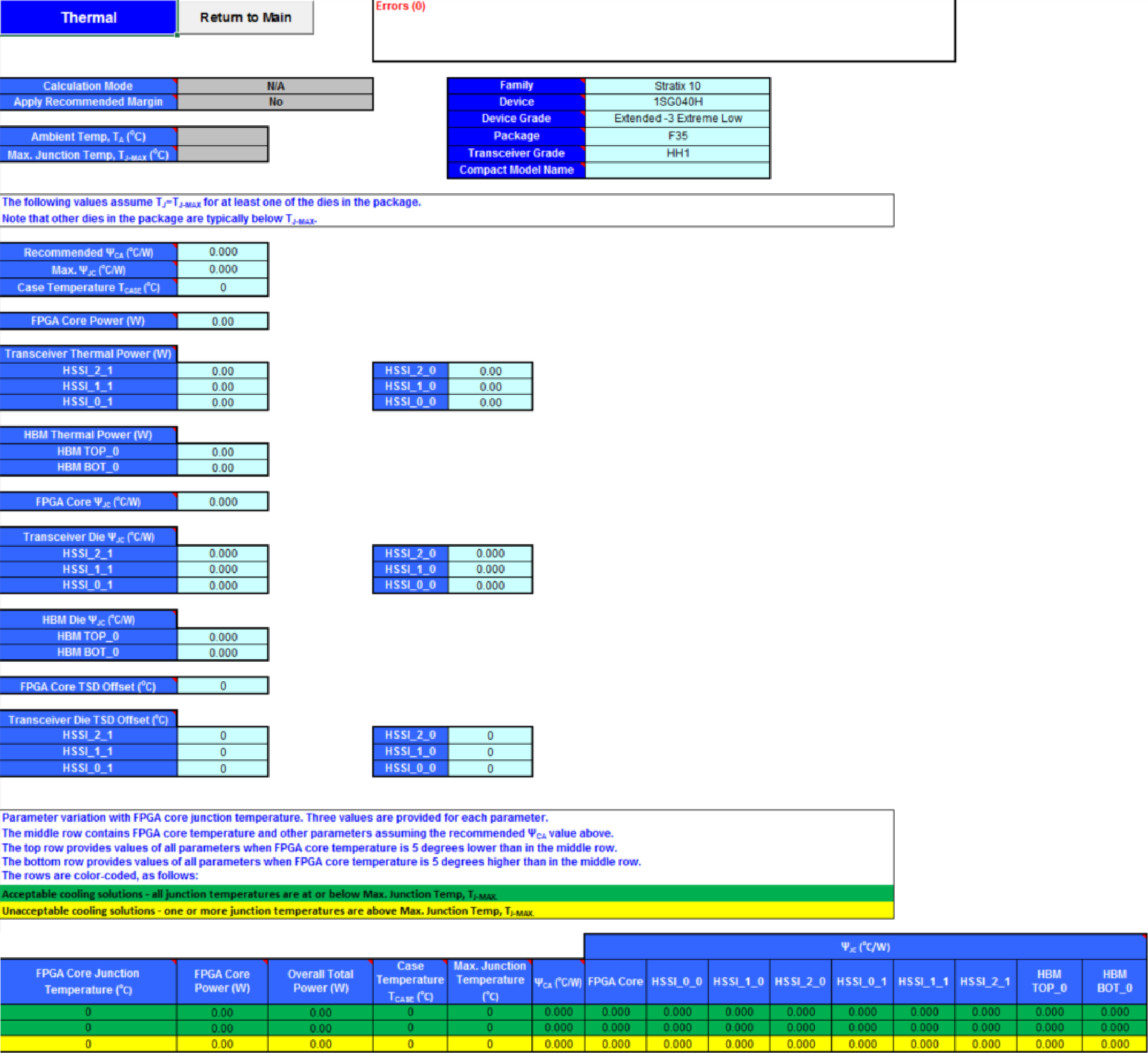
Figure 21. Intel® Stratix® 10 EPE Thermal Worksheet
| Parameter | Description |
|---|---|
| Calculation Mode | Specifies the calculation mode for the thermal solver to use. Only one calculation mode is currently supported, which determines the cooling solution required to not exceed the specified maximum junction temperature TJ.
Note: To enable the Thermal worksheet, set the Junction Temp Mode on the Main worksheet to Detailed Thermal Model.
|
| Apply Recommended Margin | Specifies whether to apply recommended margins to power estimates for thermal analysis. Recommended margins are based on power model maturity, as follows:
These margins apply only to thermal analysis results. Selecting Yes causes the total power to be higher on the Thermal worksheet than power reported elsewhere in the Early Power Estimator. |
| Ambient Temp, TA (°C) | Specify the temperature of the air that is cooling the device. |
| Max. Junction Temp, TJ-MAX (°C) | Specify the maximum junction temperature that no part of any die in the package should exceed. |
| Parameter | Description |
|---|---|
| Family | Specifies the device family selected on the Main worksheet. |
| Device | Specifies the device selected on the Main worksheet. |
| Device Grade | Specifies the device grade selected on the Main worksheet. |
| Package | Specifies the device package selected on the Main worksheet. |
| Transceiver Grade | Specifies the transceiver grade selected on the Main worksheet. |
The fields of the following table provide thermal parameters when junction temperature of at least one part of one of the dies is at the specified maximum junction temperature, provided that such a scenario is achievable using reasonable cooling solutions, given specified ambient temperature and power consumption of the design. In a typical case other dies in the package may be at a temperature lower than the specified maximum. The Early Power Estimator takes this into account when reporting power and other parameters. If the specified ambient and maximum junction temperatures are such that no reasonable cooling solution can satisfy the requirements, the EPE produces the following error on the Thermal worksheet: ERROR: Could not find a valid cooling solution for specified input parameters. If this error occurs, enter more realistic ambient and maximum junction temperatures given the power consumption of your design
| Parameter | Description |
|---|---|
| Recommended ΨCA(°C/W) | ψCA is the thermal resistance between the center of the package integrated heat spreader (IHS) and ambient temperature. The recommended ΨCA is the highest possible thermal resistance of the cooling solution that ensures no part of any die exceeds the specified maximum junction temperature. |
| Max. ΨJC(°C/W) | ψJC is the thermal resistance between each of the dies in the package and the center of the package integrated heat spreader. This field shows the maximum ΨJC among all dies, assuming the recommended ΨCA value above. |
| Case Temperature TCASE (°C) | The case temperature, which is the temperature at the top center of the integrated heat spreader, assuming the recommended ΨCA value listed above. |
| FPGA Core Power (W) | The total power consumption of the main FPGA die containing core logic, assuming the recommended ΨCA value. This power is reported at the actual temperature of the core die, assuming the recommended ΨCA value. This temperature may be equal to the maximum junction temperature if the FPGA core die is at the highest temperature among all dies (also known as a hot spot). The FPGA core may also be at a lower temperature, if the hot spot is elsewhere in the package (i.e. on another die). |
| Transceiver Thermal power (W) | The total power consumption of each transceiver die, assuming the recommended ΨCA value. This power is reported at the actual temperature of the specific die, assuming the recommended ΨCA value above. This temperature may be equal to the maximum junction temperature if a specific die is the hot spot, or it may be at a lower temperature if the hot spot is elsewhere in the package.
Note: Each transceiver die in the package reports a small amount of static power even when no channels are used in the corresponding transceiver tile and transceiver rails (VCCR_GXB, VCCT_GXB, and VCCH_GXB) of that tile are grounded. This is an expected result.
|
| HBM Thermal Power (W) | The total power consumption of each HBM die, assuming the recommended ΨCA value. This power is reported at the actual temperature of the specific die, assuming the recommended ΨCA value above. This temperature may be equal to the maximum junction temperature if a specific die is the hot spot, or it may be at a lower temperature if the hot spot is elsewhere in the package. |
| FPGA Core ψJC(°C/W) | The thermal resistance between the main FPGA core die and the center of the package integrated heat spreader, assuming the recommended ΨCA value. |
| Transceiver Die ψJC(°C/W) | The thermal resistance between each transceiver die and the center of the package integrated heat spreader, assuming the recommended ΨCA value. |
| HBM Die ψJC(°C/W) | The thermal resistance between each HBM die and the center of the package integrated heat spreader, assuming the recommended ΨCA value. |
| FPGA Core TSD Offset (°C) | The offset between the highest temperature (hot spot) of the main FPGA core die and the temperature determined by reading the temperature sensing diode (TSD) on the FPGA core die. FPGA core temperature = FPGA core TSD temperature + FPGA core TSD offset. |
The following table shows variations of thermal parameters and power consumption with changing junction temperature of the main FPGA core die. Three values are provided for each parameter. The middle row contains FPGA core temperature and other parameters assuming the recommended ΨCA value above. The top row provides values of all parameters when FPGA core temperature is 5 degrees lower than in the middle row. Similarly, the bottom row provides values of all parameters when FPGA core temperature is 5 degrees higher than in the middle row. It is important to realize that under the conditions in the last row at least one part of one die in the package exceeds the requested maximum junction temperature, and may even exceed the maximum allowed value for the device. Therefore the values in the last row should be used only as an estimate of power dependence on temperature for the purpose of computational fluid dynamic (CFD) simulation, and not for any other purpose.
| Parameter | Description |
|---|---|
| FPGA Core Junction Temperature (°C) | Shows the FPGA core die temperature for each of the three rows, as explained above. |
| FPGA Core Total Power (W) | Provides total power consumption of the main FPGA die containing core logic, assuming the specific core temperature in the given table row. |
| Overall Total Power (W) | Provides total power consumption of all dies in the package, assuming the specific core temperature in the given table row. |
| Case Temperature TCASE (°C) | Provides the case temperature, assuming the specific core temperature in the given table row. |
| ψCA (°C/W) | Provides the thermal resistance between the center of the package integrated heat spreader and the ambient temperature, assuming the specific core temperature in the given table row. For each row, this is the ΨCA value that would cause the FPGA core junction temperature to be at the specific value for a given row. |
| ψJC (°C/W) | Provides the thermal resistance between each die and the center of the package integrated heat spreader, assuming the specific core temperature in the given table row |
In extreme cases, such as thermal runaway, it may not be possible to calculate the values for +/- 5 degrees, in which case the Thermal worksheet displays the error message: ERROR: Could not calculate parameter variation with core temperature. Try adjusting TJ-MAX to obtain temperature-dependent parameters. When this error occurs, the recommended ΨCA value and all other values above are valid, but the table showing variation of thermal parameters and power consumption with changing junction temperature of the main FPGA core die contains some invalid values. As the error text indicates, adjusting the maximum junction temperature may allow the thermal solver to calculate this dependence, albeit at a different range of FPGA core temperatures than the usual range.
For more information about thermal modeling, refer to AN-787: Thermal Modeling and Management.