Visible to Intel only — GUID: ytb1555546047624
Ixiasoft
1. 25G Ethernet Intel® FPGA IP Quick Start Guide
2. 10G/25G Ethernet Single-Channel Design Example for Intel® Stratix® 10 Devices
3. 25G Ethernet Single-Channel Design Example for Intel® Stratix® 10 Devices
4. 25G Ethernet Multi-Channel Design Example for Intel Stratix 10 Devices
5. 25G Ethernet Intel® FPGA IP Design Example References
6. 25G Ethernet Intel® Stratix® 10 FPGA IP Design Example User Guide Archives
7. Document Revision History for the 25G Ethernet Intel® Stratix® 10 FPGA IP Design Example User Guide
1.1. Directory Structure
1.2. Generating the Design Example
1.3. Simulating the 25G Ethernet Intel® FPGA IP Design Example Testbench
1.4. Compiling and Configuring the Design Example in Hardware
1.5. Changing Target Device in Hardware Design Example
1.6. Testing the 25G Ethernet Intel® FPGA IP Design in Hardware
Visible to Intel only — GUID: ytb1555546047624
Ixiasoft
1.5.1. Procedure
To change the target device in your hardware design example, follow these steps:
- Launch the Intel® Quartus® Prime Pro Edition software and open the hardware test project file /hardware_test_design/eth_ex_25g.qpf.
- On the Assignments menu, click Device. The Device dialog box appears.
- In the Device dialog box, select 1SG280LU2F50E2VG (L-tile) or 1SG280HU1F50E2VG (H-tile) in the target device table that matches the device part number on your development kit. Refer to the Stratix® 10 GX Signal Integrity Development Kit link on the Intel® website for more information.
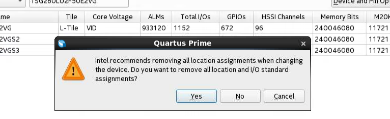
- A prompt appears when you select a device, as shown in the figure below. Select No to preserve the generated pin assignments and I/O assignments.
Figure 5. Intel® Quartus® Prime Prompt for Device Selection
- If you select 1SG280HU2F50E2VG (H-Tile GX) as your target device, click Upgrade IP Components in the Project menu, select 25G Ethernet FPGA IP from the list of IP components, and click Upgrade in Editor. Regenerate this IP component.
Note: If you select 1SG280LU1F50E2VG (L-Tile GX) as your target device, skip this step if you are using the same Quartus and IP version.
- Modify the pin assignment of cpu_resetn port to pin AW10 through Pin Planner or Assignment Editor in the Intel® Quartus® Prime Pro Edition. No other pin assignment modifications are required for the design example. When you generate the design example targeting other Intel® Stratix® 10 development kits, refer to the respective development kit user guides for pin assignment.
- Perform full compilation of your design.
You can now test the design on your hardware.