Visible to Intel only — GUID: cdm1534297447492
Ixiasoft
2.3.2.5. PCB Connector
Connectors are unavoidable in PCB board design. Hence, the PCB connector footprint must be optimized and tuned to reach the trace target impedance and have less discontinuity or reflection. Here are some tips that you can follow to optimize the PCB connector footprint:
- Optimize the PCB connector footprint while following the connector vendor’s guideline.
- Provide the PCB stackup and material information for the connector vendor to optimize the PCB footprint based on the channel impedance requirement.
- Make sure the connector model boundary is defined clearly.
- The connector model from the vendor usually includes the vendor’s reference PCB footprint.
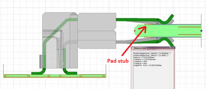
- Check if the connector model from the vendor includes the worst-case geometry, i.e. the pad stub of the mated edge card.
The following figure shows a QSFP connector as an example in the PCB connector footprint optimization.
Figure 12. QSFP Connector and PCB Footprint Optimization
Co-simulation must be done with the connector in an E/M tool solver. In the pre-layout phase, provide the PCB stackup and materials to the connector vendor for preliminary footprint optimization. In the post-layout phase, provide the routed PCB footprint to the connector vendor along with the final co-simulation with connector. Make sure to define a clear boundary for the final post-layout model for the end-to-end channel simulation.