Visible to Intel only — GUID: cfc1529450445926
Ixiasoft
5.3.2. The System Info Tab
The System Info tab shows information about the board's current configuration. The tab displays system-MAX V control setting, the board's MAC address, and other details stored on the board.
Figure 15. The System Info Tab
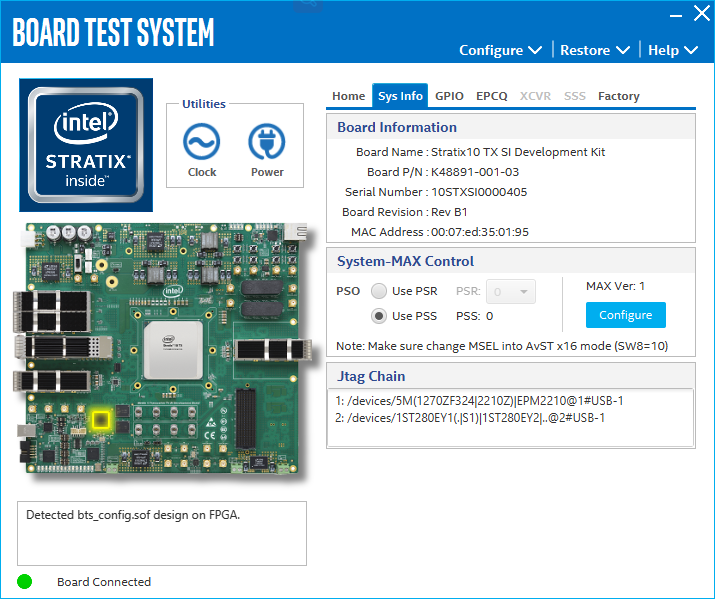
The following sections describe the controls on the System Info tab.
Board Information
The Board Information control displays static information about your board. The information is displayed after configuring the FPGA with GPIO/FLASH design.
- Board Name: Indicates the official name of the board given by the BTS.
- Board P/N: Indicates the part number of the board.
- Serial Number: Indicates the serial number of the board.
- Board Revision: Indicates the revision of the board.
- MAC Address : Indicates the MAC Address of the board.
System-MAX Control
The MAX V register control allows you to view and change the current MAX V register values as described in the table below. Change to the register values with the GUI take effect immediately.
| MAX V Register Values | Description |
|---|---|
| Configure | Resets the system and reloads the FPGA with a design from flash memory based on the other MAX V register values. |
| PSO | Sets the MAX V PSO register |
| PSR | Sets the MAX V PSR register. Allows PSR to determine the page of flash memory to use for FPGA reconfiguration. The numerical values in the list corrresponds to the page of flash memory to load during the FPGA reconfiguration. |
| PSS | Displays the MAX V PSS register value. Allows the PSS to determine the page of flash memory to use for FPGA reconfiguration. |
| MAX Ver | Indicates the version of MAX V code currently running on the board.The MAX V code resides in the <package dir>\examples\max5 directory. Newer revisions of this code may be available on the Stratix 10 Transceiver Signal Integrity Development Kit link on the Intel website. |
JTAG Chain
The JTAG chain control shows all the devices currently in the JTAG chain.
Note: When switch SW 1-2 (MAX BYPASS) is set to 1 (OFF), the JTAG chain includes the MAX V device. When set to 0 (ON), the MAX V device is removed from the JTAG chain. System MAX and FPGA must be in the JTAG chain when running the BTS GUI.