Visible to Intel only — Ixiasoft
Intel® Stratix® 10 Devices and Transceiver Channels
PCB Stackup Selection Guideline
Recommendations for High Speed Signal PCB Routing
FPGA Fan-out Region Design
CFP2/CFP4 Connector Board Layout Design Guideline
QSFP+/zSFP/QSFP28 Connector Board Layout Design Guideline
SMA 2.4-mm Layout Design Guideline
Tyco/Amphenol Interlaken Connector Design Guideline
Electrical Specifications
Document Revision History for AN 766: Intel® Stratix® 10 Devices, High Speed Signal Interface Layout Design Guideline
Option 1: Via-In-Pad Topology
Option 2: Dog-bone with GND Cutout at BGA Pad Topology
Option 3: Micro-via Topology
GND Cutout Under BGA Pads in Fan-out Configuration
Comparison of Dog-bone with GND Cutout Under the BGA and Via-in-Pad Configurations
Trace Shape Routing at the BGA Void Area (Tear Drop Configuration)
Visible to Intel only — Ixiasoft
This routing design is configured with the following characteristics:
- The stack-up is 24 layers with a thickness of 117 mil
- Eight signal layers
- Four PWR layers
- Material is Megtron6
- Via-in-pad topology with 8 mil finished drill
- 18-mil signal pad and 28 mil signal anti-pad
- Horizontal anti-pad is 68 mil (40 mil pitch + 28 mil anti-pad)
- Vertical anti-pad is 28 mil
Figure 18. Case1: Conventional Differential Routing with Neck-down and Jog-out
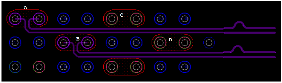
The transceiver pair of A and B have been routed on the layer 5 of stackup. Transceiver pair of C and D on the same row have been routed on a different layer. Only two signal layers are required for four transceiver pairs by using conventional differential routing with neck-down and jog-out routing.
Figure 19. Case2: Conventional Single-ended In-line Breakout Routing with Jog-out
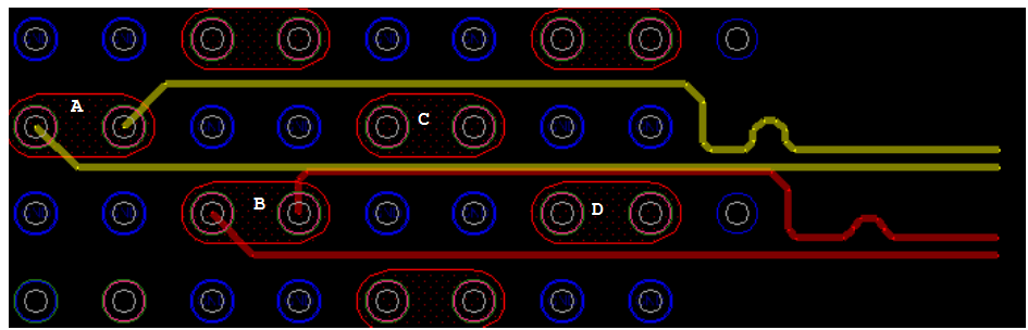
Yellow routing shows transceiver pair A routed on layer seven. Red routing shows transceiver pair B routed on layer nine. Due to single-ended break-out and lack of space, the transceiver pairs C and D on the same row have been routed on different layers. Four signal layers are required for four transceiver pairs by using conventional single-ended in-line breakout routing with jog-out.
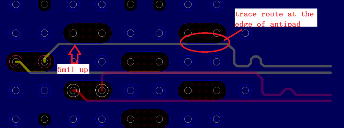
Because fabrication always has some layer-to-layer mismatch, this example implements a typical 5 mil layer-to-layer mismatch to the cases above. This allows you to observe the level of sensitivity to layer-to-layer fabrication mismatch. This layer-to-layer fabrication mismatch moves the routing passing by the GND void area and adds more discontinuity to the routing path.
Figure 20. Case 3: 5 mil Layer-to-layer Fabrication Mismatch on Conventional Differential Routing with Neck-down and Jog-out
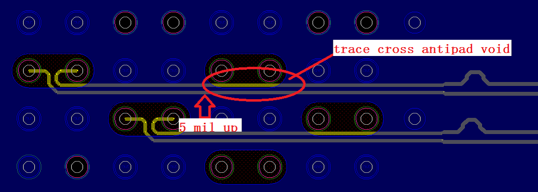
Figure 21. Case 4: 5 mil Layer-to-layer Fabrication Mismatch on Conventional Single-ended In-line Breakout Routing and Jog-out
Performance Comparison Between Case 1 and Case 3
This section compares the performances between conventional differential routing with neck-down and jog-out with/without mismatch (Case 1 vs Case 3).
Figure 22. Simulated Differential Insertion Loss

Figure 23. Simulated Differential Return Loss at the BGA Solder Ball
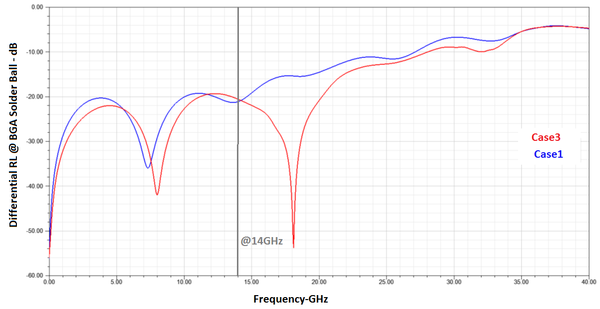
Figure 24. Simulated TDR Differential Impedance from the Trace End

These performance results demonstrate that within 15 GHz bandwidth Case1 is robust enough to accommodate the layer-to-layer fabrication mismatch. The TDR impedance shows up to 7 Ω impedance mismatch due to the 5 mil layer-to-layer mismatch.
Performance Comparison Between Case 2 and Case 4
This section compares the performances between conventional single-ended in-line routing with jog-out with/without mismatch (Case 2 vs Case 4).
Figure 25. Simulated Differential Insertion Loss
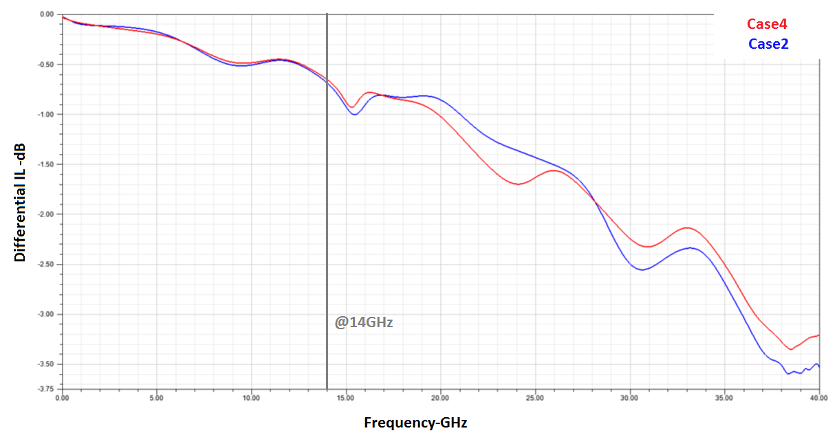
Figure 26. Simulated Differential Return Loss at BGA Solder Ball
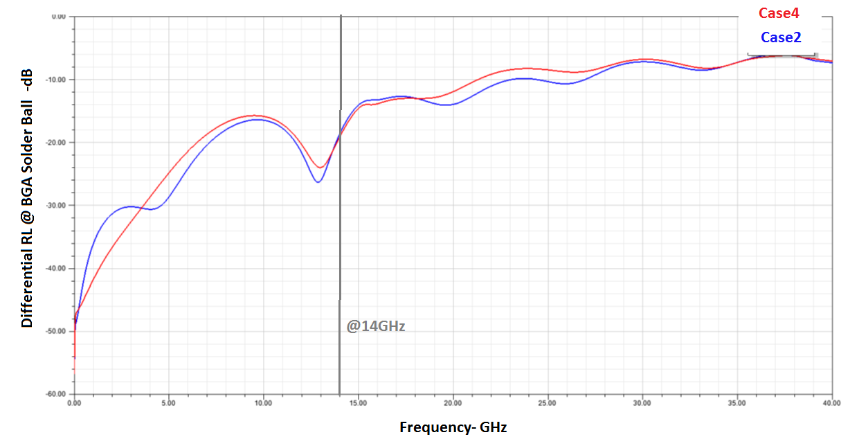
Figure 27. Simulated TDR Differential Impedance from the Trace End
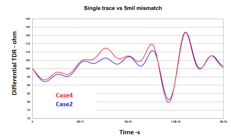
These performance results demonstrate that within 15 GHz bandwidth, Case 2 has a more robust layer-to-layer fabrication mismatch. The TDR impedance shows up to a 5Ω impedance mismatch occurring due to the 5 mil layer-to-layer mismatch.
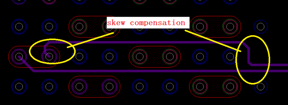
Intel recommends that the break-out routing is either differential neck-down with back-jog or single-ended bak-jog routings due to the fixed skew matching at the BGA area. The following figures demonstrate the recommended break-out routing performances.
Figure 28. Case 5: Differential Routing with Neck-down and Back-jog

Figure 29. Case 6: Single-Ended Routing with Back-jog
Performance Comparison Between Case 1 and Case 5
This section compares the performances between conventional differential routing with neck-down and jog-out and differential routing with neck-down with back-jog (Case 1 vs Case 5).
Figure 30. Simulated Differential Insertion Loss
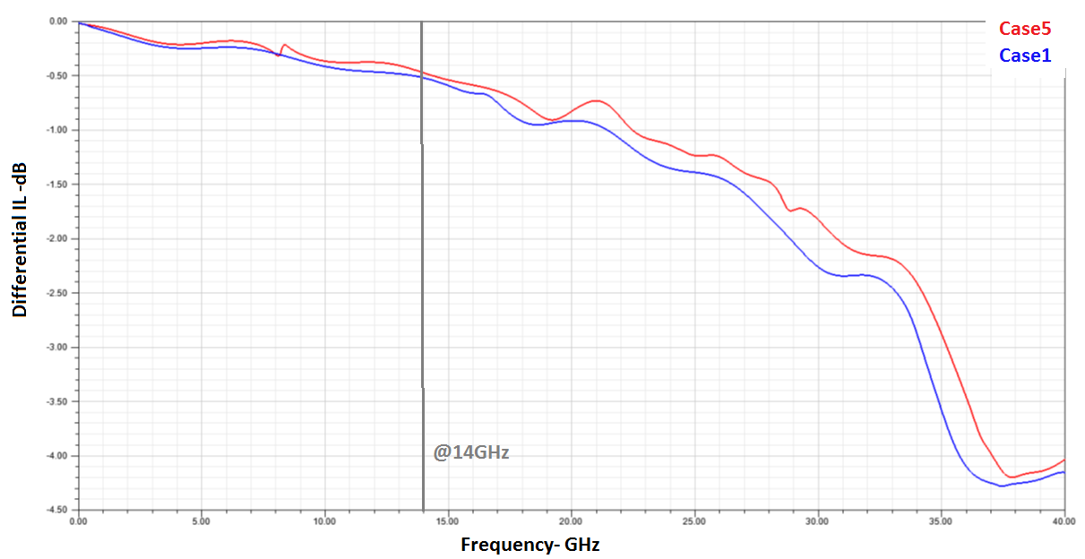
Figure 31. Simulated Differential Return Loss at the BGA Solder Ball
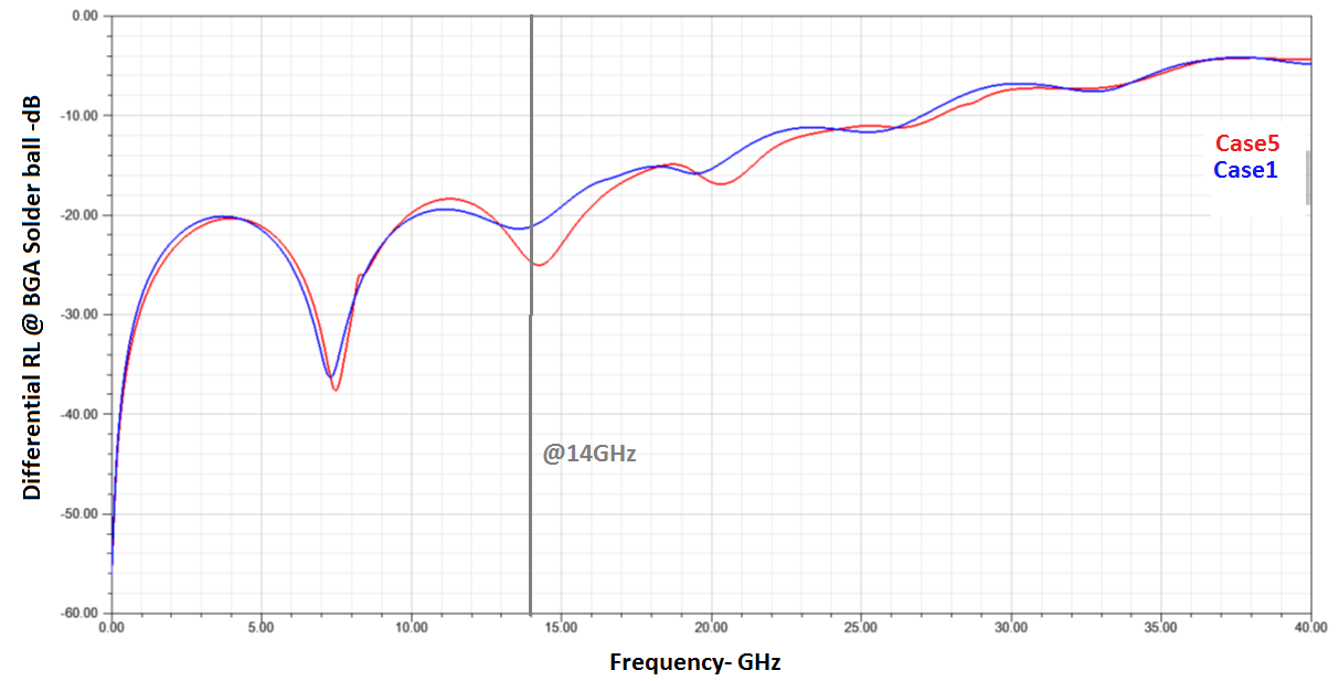
Comparing the conventional differential and jog-out routing configurations with the recommended differential routing with back-jog shows up to 0.1 dB insertion loss improvement. It also exhibits up to a 5 dB return loss improvement within a 15 GHz bandwidth when using the back-jog configuration.
Performance Comparison Between Case 2 and Case 6
This section compares the performances between conventional single-ended in-line breakout routing with jog-out and single-ended routing with back-jog (Case 2 vs Case 6).
Figure 32. Simulated Differential Insertion Loss
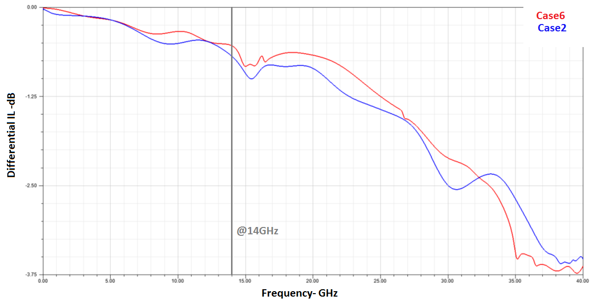
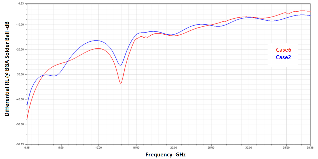
Figure 33. Simulated Differential Return Loss at the FPGA Solder Ball
Single-ended break-out routing is less sensitive to layer to layer mismatch.
Comparing the conventional single-ended routing with jog-out and the recommended single-ended routing with back-jog, the single-ended routing with back-jog shows an insertion loss improvement of up to 0.25 dB. It also exhibits a return loss improvement up to 7 dB within a 1 -GHz bandwidth.
The differential break-out routing with back-jog shows 0.1 db insertion loss improvement and up to 6 dB return loss improvement within 15 GHz bandwidth compared to single-ended break-out routing with back-jog.
In addition, differential break-out routing with back-jog has slightly better performances above 15 GHz compared to single-ended routing with back-jog.
Intel recommends use of single-ended routing with back-jog due to less sensitivity over the layer-layer mismatch, if customers use low number of transceiver channels or they have enough signal layers for routing. Due to this, differential break-out routing with back-jog is preferred to single-ended break-out routing with back-jog, because differential break-out routing requires half of routing layers used for single-ended break-out routing.