Visible to Intel only — GUID: joc1462997552128
Ixiasoft
Intel® Stratix® 10 Devices and Transceiver Channels
PCB Stackup Selection Guideline
Recommendations for High Speed Signal PCB Routing
FPGA Fan-out Region Design
CFP2/CFP4 Connector Board Layout Design Guideline
QSFP+/zSFP/QSFP28 Connector Board Layout Design Guideline
SMA 2.4-mm Layout Design Guideline
Tyco/Amphenol Interlaken Connector Design Guideline
Electrical Specifications
Document Revision History for AN 766: Intel® Stratix® 10 Devices, High Speed Signal Interface Layout Design Guideline
Option 1: Via-In-Pad Topology
Option 2: Dog-bone with GND Cutout at BGA Pad Topology
Option 3: Micro-via Topology
GND Cutout Under BGA Pads in Fan-out Configuration
Comparison of Dog-bone with GND Cutout Under the BGA and Via-in-Pad Configurations
Trace Shape Routing at the BGA Void Area (Tear Drop Configuration)
Visible to Intel only — GUID: joc1462997552128
Ixiasoft
Option 1: Via-In-Pad Topology
Intel recommends using via-in-pad technology for data rates above 15 Gbps. Use via-in-pad when you want to transfer signals from the BGA pad to the inner layers.
Figure 4. Option 1: FPGA Fan-out Configuration at Solder Ball Topology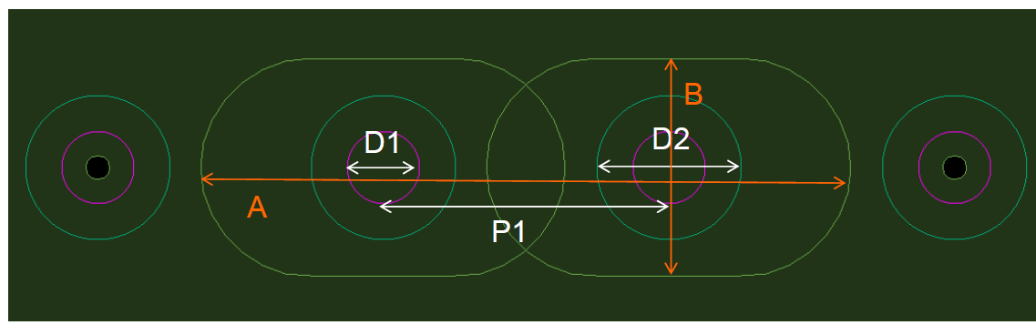
D1: Via drill hole diameter: 8 mil (for up to 1:12 stackup aspect ratio) or 10 mil for higher stackup aspect ratios.
D2: Via pad diameter: 18 mil (for up to 1:12 stackup aspect ratio) or 20 mil for higher stackup ratios.
P1: Standard via-to-via pitch: 1 mm.
A: Horizontal anti-pad: 90 mil.
B: Vertical anti-pad: 28 mil (for up to 1:12 aspect stackup ratio) or 30 mil for higher stackup aspect ratios.