Visible to Intel only — GUID: joc1463351654778
Ixiasoft
Intel® Stratix® 10 Devices and Transceiver Channels
PCB Stackup Selection Guideline
Recommendations for High Speed Signal PCB Routing
FPGA Fan-out Region Design
CFP2/CFP4 Connector Board Layout Design Guideline
QSFP+/zSFP/QSFP28 Connector Board Layout Design Guideline
SMA 2.4-mm Layout Design Guideline
Tyco/Amphenol Interlaken Connector Design Guideline
Electrical Specifications
Document Revision History for AN 766: Intel® Stratix® 10 Devices, High Speed Signal Interface Layout Design Guideline
Option 1: Via-In-Pad Topology
Option 2: Dog-bone with GND Cutout at BGA Pad Topology
Option 3: Micro-via Topology
GND Cutout Under BGA Pads in Fan-out Configuration
Comparison of Dog-bone with GND Cutout Under the BGA and Via-in-Pad Configurations
Trace Shape Routing at the BGA Void Area (Tear Drop Configuration)
Visible to Intel only — GUID: joc1463351654778
Ixiasoft
Full CFP4 Channel Analysis Design Example (Excluding the Connector)
This section illustrates a full FP4 channel simulation.
Figure 68. Full Channel CFP4 Design ExampleFigure shows FPGA to CFP4 connector, excluding the connector.
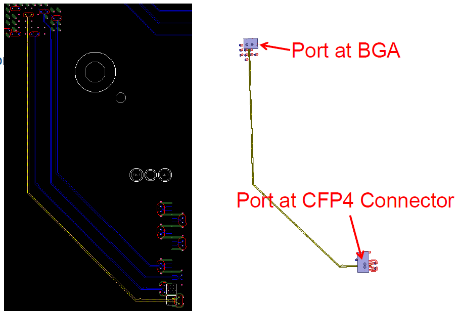
The total channel length is approximately 2.4 inch from the BGA to the connector pads.
The main routing is stripline on layer 5. The connector break-out configuration is similar to what you can see at pair 2 in .
Figure 69. Full CFP4 Channel Insertion Loss PerformanceFigure excludes the CFP4 connector.

Figure 70. Full CFP4 Channel Return Loss Performance Figure excludes the CFP4 connector.
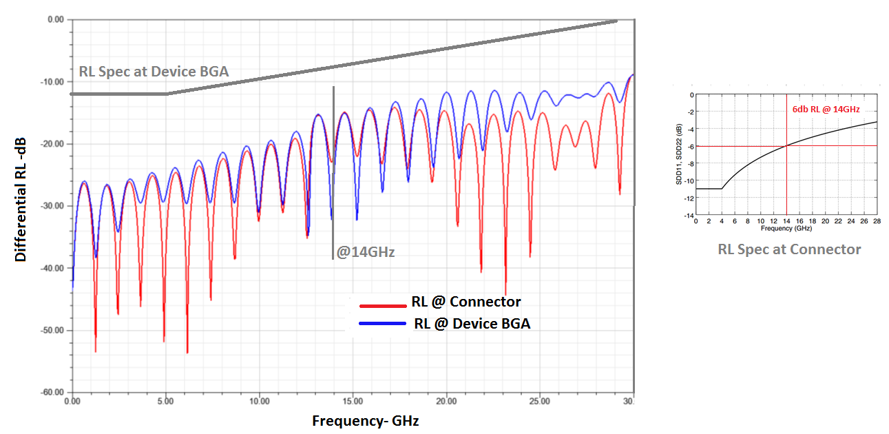
Comparing the scattering performances (SDD21 and SDD11/22) above with the host-to-module specification in CEI-28G-VSR shows that both insertion and return loss meet the specifications.