Visible to Intel only — GUID: joc1463548749547
Ixiasoft
Intel® Stratix® 10 Devices and Transceiver Channels
PCB Stackup Selection Guideline
Recommendations for High Speed Signal PCB Routing
FPGA Fan-out Region Design
CFP2/CFP4 Connector Board Layout Design Guideline
QSFP+/zSFP/QSFP28 Connector Board Layout Design Guideline
SMA 2.4-mm Layout Design Guideline
Tyco/Amphenol Interlaken Connector Design Guideline
Electrical Specifications
Document Revision History for AN 766: Intel® Stratix® 10 Devices, High Speed Signal Interface Layout Design Guideline
Option 1: Via-In-Pad Topology
Option 2: Dog-bone with GND Cutout at BGA Pad Topology
Option 3: Micro-via Topology
GND Cutout Under BGA Pads in Fan-out Configuration
Comparison of Dog-bone with GND Cutout Under the BGA and Via-in-Pad Configurations
Trace Shape Routing at the BGA Void Area (Tear Drop Configuration)
Visible to Intel only — GUID: joc1463548749547
Ixiasoft
PCB Design Guidelines for Channels with 25 Gbps + Interlaken Interface Connector Recommendations
Figure 100. TYCO Interlaken Connector GND Plane Cutout on a Host PCBH = 72.5 mil
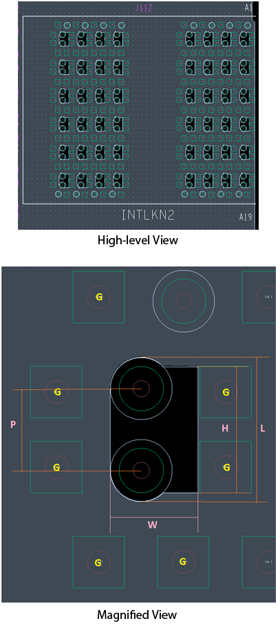
P = 47.5 mil
L = 82.5 mil
W = 52.5 mil
The maximum intra-pair skew (between P/N) is within 2 ps.
The GND reference cutout must be applied to all GND and reference planes. The dimensions of the GND cutout are 52.5 mil (W) x 72.5 mil (H).
The standard signal via used in Figure 100 has the following characteristics:
- 10 mil drill size diameter
- 26 mil pad diameter
- 36 mil anti-pad diameter
You must remove all non-functional pads.
Signal routing is differential on the main PCB before it reaches the Interlaken connector where it is turned into a single-ended routing.
Figure 101. Option 1: TYCO Interlaken Connector Routing on a Host PCB with Skew Matching50 Ω single-ended routing up to the connector edge.
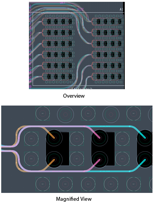
Figure 102. Option 2: Alternate TYCO Interlaken Connector Routing on a Host PCB with Skew MatchingBelow are two figures. The first one describes the use of 4 layers for routing. The second figure describes the use of two layers for routing (one layer for TX and one layer for RX for maximum isolation).
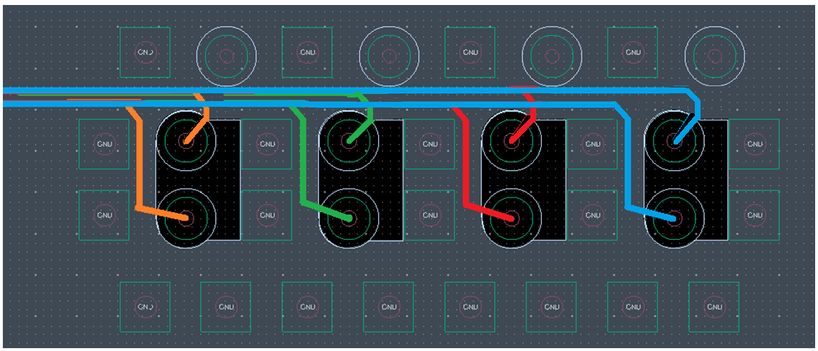
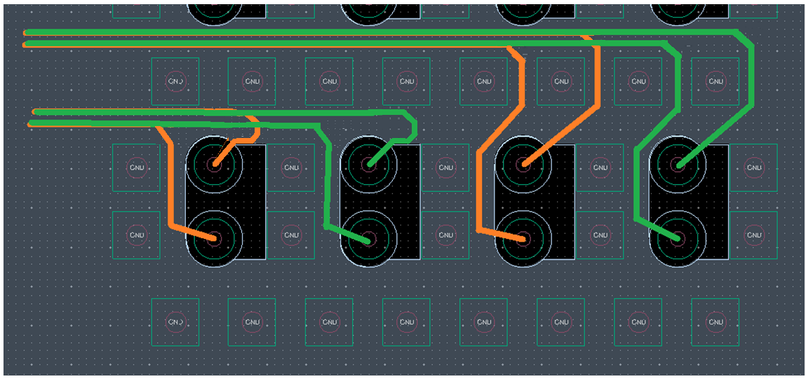
Figure 103. Interlaken Interface Connector Configurations
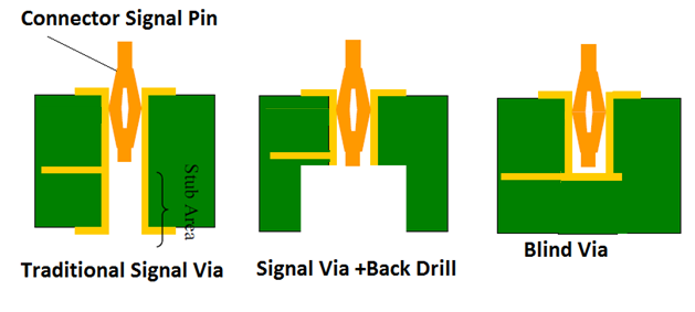
You can use either the signal via with back-drill, or a blind via at the Interlaken interface connector.
Figure 104. Recommended Routing Layer Due to the Connector Pin Length

Signal routing is located on the bottom stack-up layer to minimize the impact of stubs in the channel. Observe the following recommendations for stack-up PCB design:
- Select the appropriate stack-up. Refer to PCB Stackup Selection Guideline chapter .
- Select the PCB routing layers:
- Separate TX and RX layers for maximum isolation
- The Interlaken interface connector pins have the following lengths:
- Connector GND pin = 1.88 mm
- Connector signal pin = 1.3 mm
- Use layers below the signal pin tip for all signal routing. This helps to avoid the stub from the connector pin if the upper layers are used for routing. Use either the signal through via with back-drill or the blind via.
- Intel recommends using a 95 Ω routing trace impedance because it aligns with the following guidelines:
- For FPGA break-out, refer to FPGA Fan-out Region chapter.
- Use a 100 Ω loosely differential routing on the main host PCB if you are using option 1 in Figure 101 at the connector.
- Use a 100 Ω tightly differential routing on the main host PCB up to the connector pins if you are using option 2 in Figure 102 at the connector.
- Use the smallest routing length possible to minimize insertion loss and crosstalk.
- Ensure that all RX paths have an AC capacitor for AC coupling. Refer to the AC coupling layout design guideline in AC Coupling Capacitor Layout and Optimization Guidelines chapter.
- Ensure that you have length matching (less than 2 ps) for all TX and RX paths if this is a requirement. Refer to Recommendations for High Speed Signal PCB Routing chapter for length matching strategies at the FPGA.
- Use a back-drill for all transceiver signal vias if a through via is used.